Now Reading: What Lies Beneath the Package: A Close Look Inside Modern Chips
-
01
What Lies Beneath the Package: A Close Look Inside Modern Chips
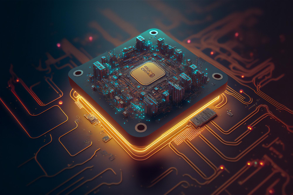
In today’s digital age, semiconductors are the silent backbone powering everything from smartphones and laptops to the most advanced data centers and AI systems. These microchips, often cloaked in innocuous packages, harbor intricate internal architectures that define their capabilities and limits. To truly appreciate how modern chips achieve astounding performance and miniaturization, we must peel back the layers—both literally and figuratively—and explore the complex world of semiconductor technology.
Unveiling the Intricacies of Modern Semiconductor Technology:
An In-Depth Examination of the Complex Layers and Components That Define Today’s Microchips and Their Impact on Computing Performance and Innovation
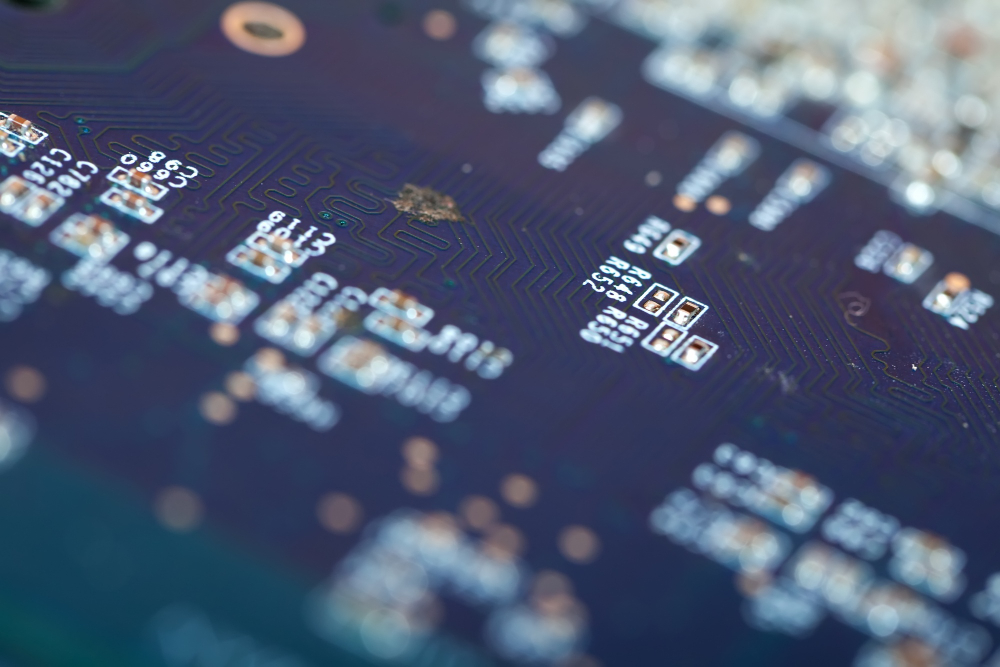
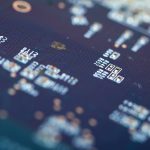
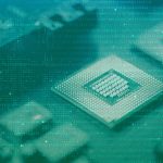
The Anatomy of a Modern Chip
At first glance, a microchip appears as a simple rectangular piece of silicon. But beneath this surface lies a densely packed Universe of layers, each with a precise function contributing to the overall operation of the device.
1. The Silicon Substrate
The foundation of any integrated circuit is the silicon wafer, a purified crystalline form of silicon. Silicon’s semiconductor properties make it ideal for controlling electrical current flow, enabling the fundamental logic operations inside chips.
2. The Dielectric Layers
Thin layers of insulating material, typically silicon dioxide or high-k dielectrics, isolate different conducting components. These layers prevent unwanted electrical interactions, maintaining signal integrity and allowing the delicate flow of electrons where needed.
3. Transistor Arrays
The core active components within a chip are transistors, primarily metal-oxide-semiconductor field-effect transistors (MOSFETs). Modern chips contain billions to trillions of these miniature switches, each precisely fabricated to turn on or off, representing binary data.
4. Interconnects
Copper or sometimes advanced materials form the conductive pathways that carry signals between transistors. The complexity and density of interconnect layers directly influence a chip’s speed and power efficiency.
5. Memory Elements
Many modern chips integrate embedded memory, such as SRAM or DRAM, within the logic layers to facilitate faster data access and reduce latency.
The Impact on Performance and Innovation
The design and fabrication of these layers directly impact a chip’s speed, power consumption, heat generation, and manufacturing costs. For instance, reducing the size of individual transistors through process nodes (measured in nanometers) allows higher transistor densities, which in turn lead to faster and more energy-efficient devices. As demands for computational power grow—driven by AI, machine learning, and high-speed data processing—these layered architectures are continually evolving to meet new challenges.
The Role of Advanced Materials
Beyond silicon, researchers are exploring new materials like graphene, transition metal dichalcogenides, and heterostructures to create transistors that push beyond the limitations of traditional semiconductors. These innovations hold the promise of faster, smaller, and more versatile chips.
Deep Dive into the Architecture and Fabrication of Contemporary Chips:
Exploring the Sophisticated Design Principles, Material Science, and Manufacturing Processes That Enable the Miniaturization, Efficiency, and Advanced Functionality of Modern Integrated Circuits and Their Role in Shaping the Future of Electronics
Design Principles of Modern Chips
Today’s microarchitectures rely heavily on modularity, parallelism, and scalability. Engineers utilize hardware description languages and computer-aided design (CAD) tools to optimize the arrangement of millions of transistors.
System-on-Chip (SoC) architectures integrate multiple functionalities—CPU, GPU, memory controllers, I/O interfaces—into a single silicon piece, reducing latency and power consumption while saving space.
Fabrication Processes: From Silicon Wafers to Tiny Transistors
The creation of a modern chip involves a series of highly precise and complex steps:
- Photolithography: Using ultraviolet light and masks to transfer circuit patterns onto silicon wafers. The trend toward extreme ultraviolet (EUV) lithography enables patterning at sub-7nm nodes, essential for manufacturing ever-smaller transistors.
- Doping: Introducing impurities into silicon to modify electrical properties, creating regions of p-type and n-type silicon needed for transistor action.
- Etching and Deposition: Removing material or adding thin films layer-by-layer to build up the complex multilayered structures within the chip.
- Chemical-Mechanical Planarization (CMP): Smoothing layers to ensure uniformity for subsequent patterning steps.
Achieving Miniaturization and Efficiency
Shrinking transistor sizes—down to the nanometer scale—allows for greater transistor density, shorter electrical paths, and reduced power leakage. These advancements are key to enabling faster processing speeds and lower energy consumption.
Advanced Packaging: Beyond individual transistor fabrication, modern manufacturing emphasizes sophisticated chip packaging, such as 3D stacking and chiplets, to enhance bandwidth and efficiency while maintaining compact form factors.
The Future of semiconductor manufacturing
Continued progress hinges on overcoming physical and economical challenges associated with further shrinking devices. Innovations like gate-all-around (GAA) transistors, new materials, and alternative architectures (like quantum dots or neuromorphic chips) are actively under development to sustain Moore’s Law and meet the demands of future computing paradigms.
Concluding Thoughts
Peering inside a modern chip reveals a marvel of engineering, material science, and manufacturing prowess. The layers and components work in harmony, pushing the boundaries of what’s possible in electronics and computing. As technology advances, understanding the intricacies beneath the package helps us appreciate the remarkable science and innovation shaping our connected world—and prepares us for the even more sophisticated and powerful chips of tomorrow.