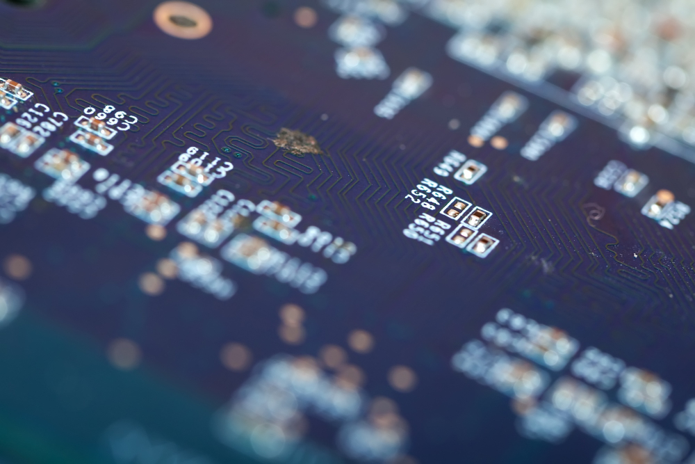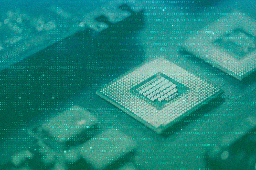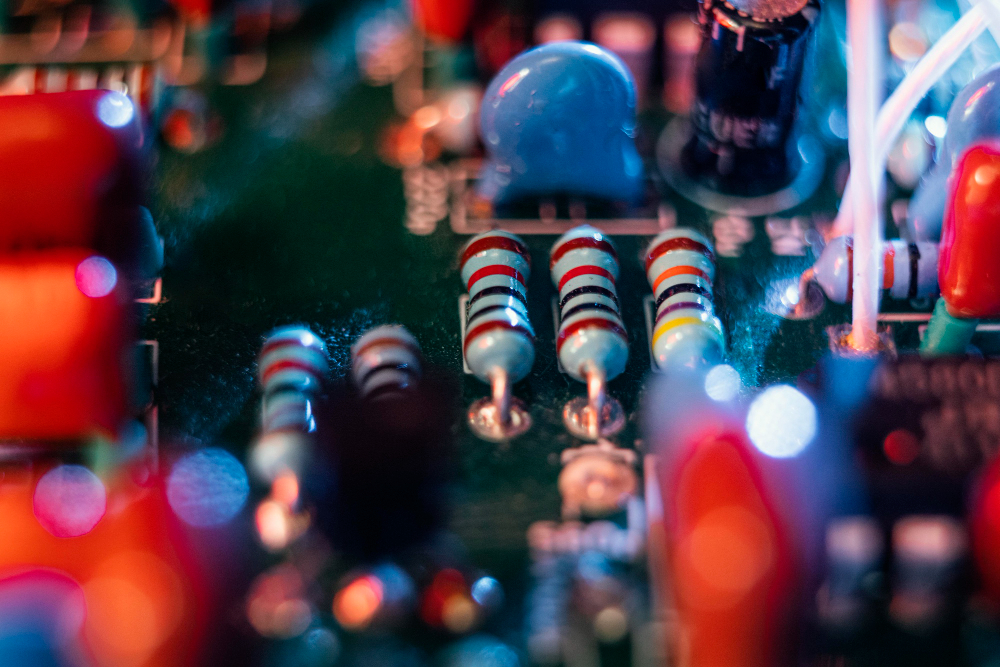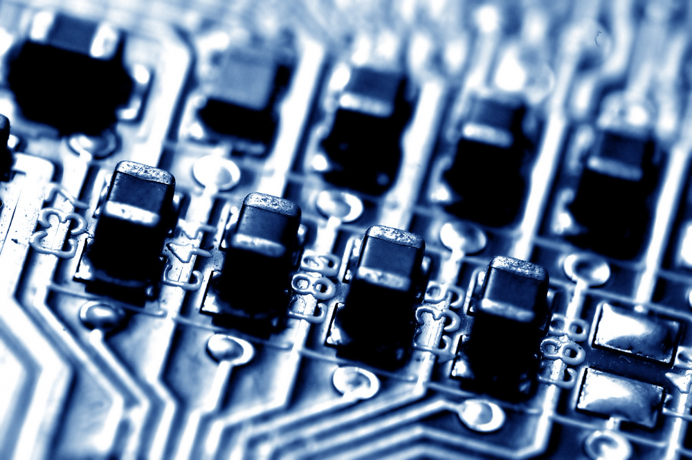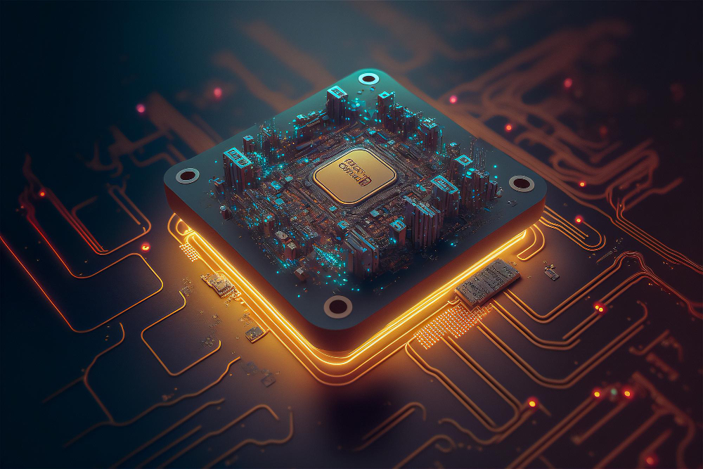
Imagine trying to coordinate a dance performance without a common beat—it wouldn't matter how talented the dancers are, without a shared sense of timing, the choreography would quickly fall apart. This analogy mirrors how electronic chips manage timing inside their circuits: by employing devices known as timers, counters, and phase-locked loops (PLLs). These tiny yet critical components work behind the scenes to ensure everything from your smartphone to complex computing systems operate seamlessly and synchronously. At the heart of many digital systems are timers. Think of a timer as a stopwatch embedded within the chip. They are designed to generate precise time intervals, often used to control event durations or to measure elapsed time. For example, in a microcontroller, a timer might be set to generate an interrupt every millisecond, which serves as a heartbeat to coordinate tasks. Timers can be simple countdown devices or sophisticated modules with features like auto-reload, prescaling, and waveform generation. They are fundamental in tasks like generating accurate delays, Pulse Width Modulation signals for controlling motors and LEDs, or creating precise timing pulses for communication protocols. Counters, on the other hand, are devices that keep track of the number of events—like how many times a button has been pressed or how many pulses have been received from a sensor. They are capable of counting edges in signals, which makes them essential in frequency measurement and event counting applications. For instance, in a digital voltmeter, counters tally the number of voltage cycles to estimate a reading. Counters can be configured to operate in binary, BCD, or other counting modes, often working in tandem with timers. Combined, these tools create intricate timing schemes that synchronize complex processes, ensuring that multiple components of a system work in harmony. While timers and counters handle quantifying and measuring time and events, phase-locked loops (PLLs) are key to generating and maintaining stable clock signals. A PLL is a feedback control system that synchronizes an output oscillator with a reference signal in frequency and phase. This means if a chip receives a 10 MHz reference clock, a PLL can produce a stable, higher-frequency clock—say 200 MHz—by continuously adjusting its internal oscillator to match the phase of the reference. PLLs are vital for frequency synthesis, clock generation, and jitter reduction. For example, in high-speed data communication, PLLs ensure the transmitted and received signals are phase-aligned, minimizing errors and maximizing data throughput. Together, these components—timers, counters, and PLLs—form the foundation of timing control in digital circuits. They enable devices to operate with precision, whether it’s in synchronizing data streams, managing power consumption, or coordinating complex computations. As technology advances, these timing mechanisms become even more sophisticated, incorporating digital signal processing techniques, adaptive algorithms, and low-power designs. Their continuous evolution enhances the reliability, speed, and efficiency of modern electronic devices. In essence, keeping track of time in electronic chips is much like conducting a well-orchestrated symphony—each timer, counter, and PLL plays a vital role in maintaining rhythm, harmony, and harmony across countless applications that define our digital world. Without these tiny but mighty components diligently counting and synchronizing, the complex dance of modern electronics would be chaotic and unreliable.