Articles

10Articles

Articles2 days ago

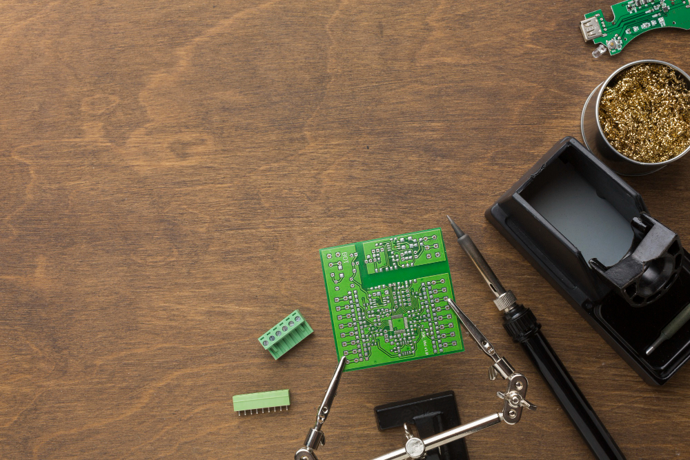
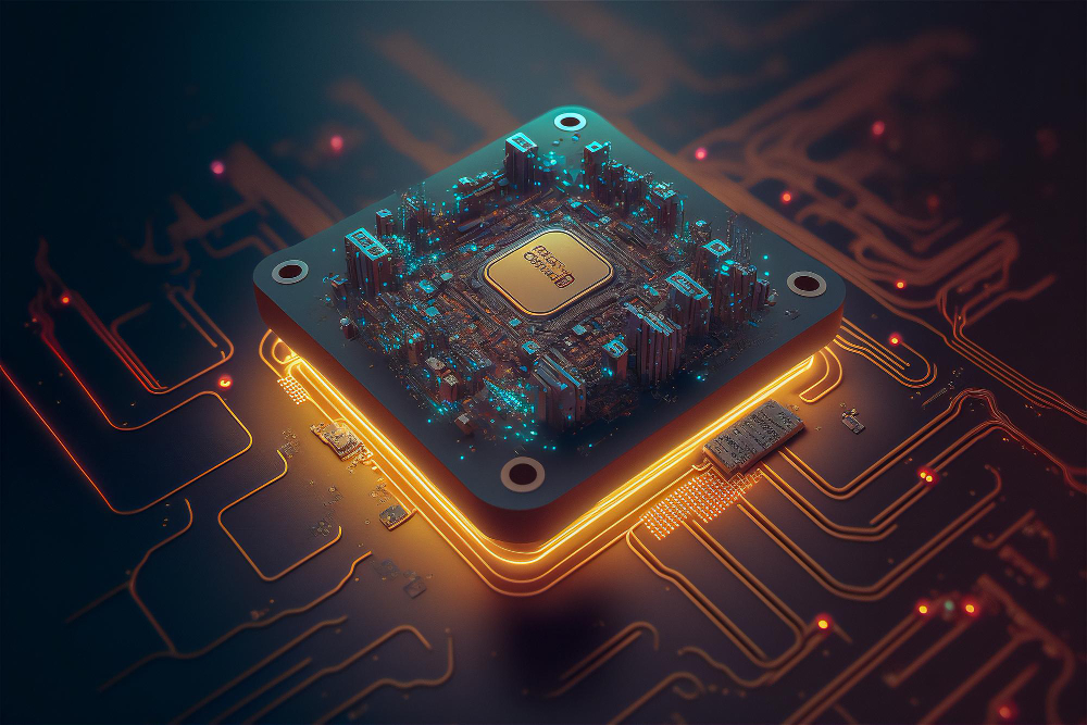
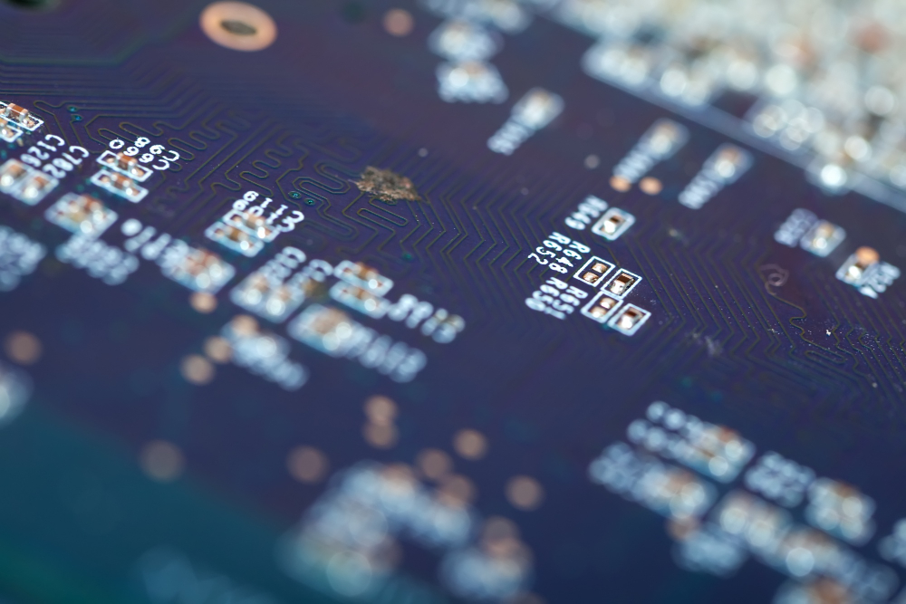
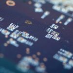
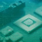
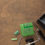
In the rapidly evolving landscape of technology, where devices become increasingly compact and integrated, the principle of minimalism has surfaced as a guiding beacon for hardware designers. "Microchip Minimalism: The Art of Elegant Hardware Design" explores how simplifying microchip architecture not only enhances performance but also achieves a harmony of form and function that appeals to both engineers and end-users. At its core, minimalism in microchip design isn’t merely about shrinking components; it’s about thoughtful engineering—eliminating unnecessary complexity, streamlining pathways, and focusing on core functionalities that deliver maximum efficiency. One of the fundamental philosophies behind this approach is the acknowledgment that less is often more. By reducing the number of transistors, layers, and interconnections, designers can create more reliable, energy-efficient chips that are easier to manufacture and maintain. This drive toward simplicity leads to hardware that boasts lower power consumption, reduced heat generation, and shorter production cycles—all critical factors in today’s competitive tech environment. For instance, the trend toward minimalist microcontrollers has led to devices that can run longer on smaller batteries, opening doors for more sustainable, portable, and wearable technologies. The artistry in elegant hardware design also lies in selecting the right features and integrating them seamlessly. Instead of packing microchips with a multitude of functionalities that may rarely be used, the minimalist approach emphasizes purpose-driven architecture. This means developers prioritize essential features, streamline data pathways, and optimize for specific applications. For example, in Internet of Things (IoT) devices, a simplified microchip might focus solely on sensor data collection and low-power communication, eliminating superfluous modules that could increase complexity and power drain. Such targeted design results in more reliable devices, less susceptibility to errors, and simplified debugging processes. Furthermore, the aesthetic appeal of minimalism extends beyond functionality to how the hardware is conceptualized and laid out. Compact, clean circuit designs not only look appealing but also facilitate heat dissipation and reduce electromagnetic interference. Thoughtful placement of components and intuitive routing of circuitry contribute to this elegance, emphasizing clarity and precision. These design choices echo minimalist art, where every line and space has intended purpose, creating a balanced and harmonious composition. Technological advancements have played a significant role in enabling microchip minimalism. Innovations in silicon fabrication, such as smaller process nodes, allow for more transistors to fit in a smaller area, making intricate yet efficient designs feasible. Additionally, sophisticated design tools and simulation software assist engineers in visualizing and optimizing layouts before manufacturing begins. This synergy between technological capabilities and design philosophy fosters a new era of hardware that is not only powerful but also elegantly simple. However, embracing minimalism in microchip design isn’t without challenges. It requires meticulous planning and a deep understanding of the intended application to identify what features are truly necessary. Striking the right balance between simplicity and functionality demands creativity and experience. For example, while a minimalist microchip may excel in energy efficiency and reliability, it must also meet user expectations for speed and versatility. Achieving this balance involves iterative testing, close collaboration among multidisciplinary teams, and an openness to innovative solutions that challenge conventional wisdom. In essence, microchip minimalism is an art form that exemplifies the beauty of restraint and purposeful creation. It encourages engineers to look beyond the allure of complexity and to focus on what truly matters—delivering high-performance hardware that is elegant in both form and function. As technology continues to advance, this refined approach promises to drive the development of smarter, more sustainable, and aesthetically pleasing devices that seamlessly integrate into our daily lives. Embracing minimalism in hardware is not just a trend but a fundamental shift toward creating technology that is as thoughtful and refined as the human experience it aims to augment.

Articles2 days ago

In an age dominated by sleek screens, sophisticated algorithms, and cloud computing, it’s easy to assume that the magic behind modern technology lies solely in complex software and high-level programming. Yet, at the very foundation of all these advanced systems are simple, elegant circuits that perform fundamental tasks with remarkable reliability. These basic building blocks—comprising switches, resistors, capacitors, and transistors—operate without a single line of code, yet they are instrumental in powering the complex devices we use daily. The concept of "logic without code" might seem counterintuitive at first glance. After all, code is typically associated with the control and decision-making aspects of technology, guiding machines to perform desired functions. But the essence of this idea is that, at a fundamental level, logical operations are executed through physical arrangements of simple electronic components. These components, through their states and connections, embody decision-making processes that are the backbone of digital logic. Take the classic example of a simple light switch. When you flip the switch, you are essentially toggling a circuit between two states—on or off. This binary state forms the foundation of digital logic, where circuits operate on signals representing 1s and 0s. Building upon this principle, engineers developed logic gates—AND, OR, NOT, NAND, NOR, XOR—that combine these binary signals in specific ways to perform complex operations. These gates are the core of digital electronics, enabling everything from calculators to smartphones to spacecraft navigation systems. One might wonder how such straightforward components can enable the sophisticated functionalities seen today. The answer lies in how these logic gates are interconnected to form more complex circuits, such as flip-flops, registers, and microprocessors. For example, a microprocessor—the brain of a computer—contains millions of transistors arranged in intricate configurations to carry out billions of calculations per second. This complexity is achieved not by adding more advanced individual components but by creatively connecting simple logic elements in a precise manner. Furthermore, this approach exemplifies the power of abstraction. While high-level programming languages let us write commands with human-readable syntax, at their core, executing those commands boils down to countless binary operations conducted by these simple circuits. In fact, at the chip level, every instruction executed by a modern computer is ultimately represented as a series of logical decisions made by these fundamental components. This seamless transition from simple circuits to complex behaviors demonstrates that the core principles of logic are remarkably versatile and scalable. A fascinating aspect of these simple circuits is their robustness. Because they are based on physical states—either conducting or non-conducting—they tend to be highly reliable and predictable. This is why digital systems have become the de facto standard in critical applications like aerospace, medical devices, and financial systems, where errors can have serious consequences. Despite their simplicity, these circuits exert a profound influence on the operation of complex devices, highlighting that sometimes, straightforward principles, applied cleverly, can underpin extraordinary technological achievements. In essence, understanding how simple circuits power complex devices offers a deeper appreciation for the elegance of electronic design. It reveals that at the heart of every smartphone, every computer, and even the most advanced robotics, lies a network of straightforward logic operations meticulously orchestrated to create extraordinary functionality. This realization not only underscores the importance of fundamental electronics but also inspires innovation—showing that even the simplest components, when combined thoughtfully, can solve some of the most intricate problems we face in technology today.

Articles2 days ago

Imagine trying to coordinate a dance performance without a common beat—it wouldn't matter how talented the dancers are, without a shared sense of timing, the choreography would quickly fall apart. This analogy mirrors how electronic chips manage timing inside their circuits: by employing devices known as timers, counters, and phase-locked loops (PLLs). These tiny yet critical components work behind the scenes to ensure everything from your smartphone to complex computing systems operate seamlessly and synchronously. At the heart of many digital systems are timers. Think of a timer as a stopwatch embedded within the chip. They are designed to generate precise time intervals, often used to control event durations or to measure elapsed time. For example, in a microcontroller, a timer might be set to generate an interrupt every millisecond, which serves as a heartbeat to coordinate tasks. Timers can be simple countdown devices or sophisticated modules with features like auto-reload, prescaling, and waveform generation. They are fundamental in tasks like generating accurate delays, Pulse Width Modulation signals for controlling motors and LEDs, or creating precise timing pulses for communication protocols. Counters, on the other hand, are devices that keep track of the number of events—like how many times a button has been pressed or how many pulses have been received from a sensor. They are capable of counting edges in signals, which makes them essential in frequency measurement and event counting applications. For instance, in a digital voltmeter, counters tally the number of voltage cycles to estimate a reading. Counters can be configured to operate in binary, BCD, or other counting modes, often working in tandem with timers. Combined, these tools create intricate timing schemes that synchronize complex processes, ensuring that multiple components of a system work in harmony. While timers and counters handle quantifying and measuring time and events, phase-locked loops (PLLs) are key to generating and maintaining stable clock signals. A PLL is a feedback control system that synchronizes an output oscillator with a reference signal in frequency and phase. This means if a chip receives a 10 MHz reference clock, a PLL can produce a stable, higher-frequency clock—say 200 MHz—by continuously adjusting its internal oscillator to match the phase of the reference. PLLs are vital for frequency synthesis, clock generation, and jitter reduction. For example, in high-speed data communication, PLLs ensure the transmitted and received signals are phase-aligned, minimizing errors and maximizing data throughput. Together, these components—timers, counters, and PLLs—form the foundation of timing control in digital circuits. They enable devices to operate with precision, whether it’s in synchronizing data streams, managing power consumption, or coordinating complex computations. As technology advances, these timing mechanisms become even more sophisticated, incorporating digital signal processing techniques, adaptive algorithms, and low-power designs. Their continuous evolution enhances the reliability, speed, and efficiency of modern electronic devices. In essence, keeping track of time in electronic chips is much like conducting a well-orchestrated symphony—each timer, counter, and PLL plays a vital role in maintaining rhythm, harmony, and harmony across countless applications that define our digital world. Without these tiny but mighty components diligently counting and synchronizing, the complex dance of modern electronics would be chaotic and unreliable.

Articles2 days ago

In the realm of electronics, the pursuit of perfection has often driven engineers and scientists to push the boundaries of what’s possible. For decades, the goal was simple: create signals that are as clean and error-free as possible, with minimal noise or distortion. But as technology has advanced and our devices have become more sophisticated, a new understanding has emerged. Perfect signals, it turns out, do not truly exist, and perhaps never will. Instead, the focus has shifted toward mastering the art of noise shaping, a technique that allows us to control and distribute unwanted noise in ways that enhance overall system performance. Noise shaping is a concept deeply rooted in the principles of signal processing, especially in analog-to-digital and digital-to-analog conversion. The idea is not to eliminate noise altogether—an impossible task—but to manipulate its spectral distribution so that it becomes less perceptible or less disruptive to the intended signal. Think of it like a finely tuned audio equalizer that pushes undesirable frequencies into regions where they are less noticeable, or into frequency bands that can be filtered out more easily. This strategic redistribution of noise allows electronic devices to perform at levels that were once considered unattainable, delivering clearer audio in smartphones, more accurate measurements in scientific instruments, and smoother data streams in high-speed communications. Modern noise shaping techniques have become foundational in many cutting-edge technologies. For instance, delta-sigma modulators, widely used in audio DACs (digital-to-analog converters), employ high-order noise shaping to push quantization noise out of the audible range. This process results in remarkably high-fidelity sound reproduction from relatively inexpensive components. Similarly, in data storage and transmission, noise shaping enhances the signal-to-noise ratio, enabling higher data rates and more reliable communications without requiring prohibitively expensive hardware. One of the most fascinating aspects of noise shaping is its philosophical shift away from perfection toward optimization. Instead of striving for absolutely pristine signals—which, due to physical limitations and quantum effects, is fundamentally impossible—researchers aim to make noise less intrusive and more manageable. This is where the concept of psychoacoustics becomes essential. By understanding how humans perceive sound, engineers can design noise shaping algorithms that mask or diminish noise in ways that are virtually imperceptible to the human ear. This synergy of human perception and engineering innovation has led to consumer electronics with audio quality that surpasses expectations, despite the underlying presence of noise. Furthermore, noise shaping contributes significantly to the ongoing miniaturization and efficiency of electronic components. As devices shrink and power constraints tighten, the ability to manage noise effectively ensures that performance does not suffer. For example, in RF (radio frequency) systems, noise shaping helps maintain signal integrity over long distances or in noisy environments, extending communication reach and reliability. It also plays a critical role in emerging fields like quantum computing and nanoscale electronics, where physical and quantum noise sources are inherently significant, demanding sophisticated approaches to noise management. Despite its many advantages, noise shaping is not without challenges. Designing high-order filters and modulators requires complex algorithms and extensive computational resources. Precision is key; even tiny deviations can lead to increased noise or signal distortion. Researchers continuously seek novel methods, such as machine learning-enhanced algorithms, to refine noise shaping techniques further. This ongoing innovation underscores a fundamental truth in electronics: perfection is a moving target, but mastery over imperfection—via noise shaping—is the path forward. In essence, the realization that perfect signals don’t exist has liberated the field of electronics from its impossible quest for flawlessness. Instead, it has opened the door to a more pragmatic and sophisticated approach—one that accepts, manages, and even leverages noise to improve device performance. Noise shaping exemplifies this mindset beautifully, transforming an unavoidable byproduct into a secret weapon for the future of technology. As researchers continue to explore and refine these methods, we can expect electronic systems that are more efficient, more resilient, and more in tune with the complex, imperfect world they inhabit. The future isn’t about eliminating noise entirely but about understanding and directing it—making noise shaping the cornerstone of next-generation electronics innovation.

Articles2 days ago

In today's rapidly advancing technological landscape, microchips form the invisible backbone of virtually every device we rely on. From smartphones and laptops to autonomous vehicles and medical equipment, these tiny but mighty components power the modern world. Yet, behind their sleek exterior lies an intricate tapestry of engineering marvels, material science, and manufacturing precision that often goes unnoticed. Understanding what lies beneath the package of a modern chip reveals not just the complexity of these devices, but also the incredible sophistication that enables their functionality. At the heart of a typical semiconductor chip is the silicon wafer—a thin slice of high-purity silicon crystal that serves as the foundation for intricate circuitry. The process begins with photolithography, where ultraviolet light transfers microscopic patterns onto the wafer's surface, defining the pathways and components of the integrated circuit. This process, repeated multiple times with layers of conductive and insulating materials, results in the complex web of transistors, resistors, and capacitors that give the chip its processing power. Today’s chips contain billions of transistors, each just a few nanometers in size, packed together to perform millions of operations per second. These transistors act as tiny switches, switching on and off millions of times a second to execute computations. But what truly brings these circuits to life is the precise layering and doping processes that manipulate electrical properties at the microscopic level. Doping introduces impurities into silicon to enhance its conductivity, creating regions of positive or negative charge—p-type or n-type—crucial for forming the transistors' junctions. The result is a highly controlled environment where electron flow can be manipulated with extraordinary precision. This level of control is essential for the chip's efficiency, speed, and power consumption. Encasing these intricate circuits is the package—a protective shell that shields the fragile internal components from environmental damage, heat, and mechanical stress. Modern chip packages are marvels of engineering in their own right. They often comprise multiple layers, including a substrate, bonding wires, and a heat spreader. The substrate, usually made of ceramic or plastic, provides structural support and electrical connections, while bonding wires or solder bumps connect the internal silicon die to external circuitry. As devices have demanded higher performance and miniaturization, packaging technology has evolved to include ball grid arrays (BGAs) and flip-chip designs, which allow for a greater number of connections in a smaller footprint. One of the most critical aspects of modern chips is heat management. With billions of transistors operating simultaneously, thermal dissipation becomes an engineering challenge. Advanced cooling techniques, including heat sinks, vapor chambers, and even embedded microfluidic channels, are integrated within the packaging to maintain optimal operating temperatures. Without effective heat dissipation, chips risk overheating, which can lead to malfunction or reduced lifespan. Beyond the physical structures, the materials used in chip manufacturing continue to evolve. Researchers are exploring alternatives like graphene and transition metal dichalcogenides for future transistors, promising even smaller, faster, and more energy-efficient devices. Interconnects—a network of tiny copper or aluminum wires—are also being refined for lower resistance and higher data throughput, essential for keeping pace with growing data demands. The leap from basic microprocessors to today's advanced chips has been driven by innovations across multiple domains—material science, nanotechnology, and precision manufacturing. Each layer, each connection, and each minute element work together seamlessly, enabling the powerful computational capabilities we have come to depend on. Peering inside a modern chip reveals a marvel of engineering that marries the microscopic with the macro, turning what appears to be simple silicon into the engines of modern innovation. Understanding these inner workings not only sheds light on the marvels of tomorrow’s technology but also underscores the complexity and ingenuity behind the devices that have become integral to our daily lives.

Articles2 days ago

Over the past five decades, the evolution of digital logic has not only reshaped the way technology integrates into our daily lives but has also driven a relentless march forward in computing power, miniaturization, and energy efficiency. The journey from transistor-transistor logic (TTL) to complementary metal-oxide-semiconductor (CMOS) technology exemplifies a remarkable story of innovation, perseverance, and the continuous pursuit of better performance. It is a narrative intertwined with the rapid advancements in semiconductor fabrication, shifting industry standards, and the expanding scope of applications that rely on digital processing. The origins of digital logic date back to the early days of electronic computing, with TTL emerging as a dominant technology during the 1960s. TTL circuits, built with bipolar junction transistors, were praised for their speed and robustness. They provided reliable logic gates that formed the backbone of early computers and digital systems. Still, their limitations in power consumption and heat dissipation soon prompted engineers and researchers to seek alternative solutions. The increasing complexity of digital systems required more compact, energy-efficient, and scalable technologies. Enter CMOS technology in the late 1960s and early 1970s. Initially developed for commercial purposes and consumer electronics, CMOS quickly gained popularity because of its significantly lower power consumption compared to TTL. Unlike TTL devices, which drew a constant amount of current even when idle, CMOS circuits only consume power during switching events. This characteristic became increasingly vital as the number of transistors on integrated circuits ballooned into the millions and eventually billions. The shift to CMOS facilitated the development of highly integrated chips, such as the microprocessors that now serve as the brains of computers, smartphones, and countless other devices. The transition from TTL to CMOS was not merely a change in technology but also a catalyst for transformative innovations across the electronics industry. CMOS's low power consumption allowed for longer battery life in portable devices, making mobile technology a practical reality. Its scalability enabled the relentless miniaturization epitomized by Moore's Law, fueling the exponential growth of transistor density on chips. As transistor sizes shrank from micron to nanometer scales, CMOS technology incorporated advanced fabrication techniques, such as photolithography and doping processes, to push the boundaries of speed and density. Moreover, CMOS's adoption encouraged the development of complex logic families and integrated circuit architectures, which in turn opened doors for more sophisticated functionalities. Complex logic operations, digital signal processing, and memory integration all became feasible within a single chip, drastically reducing size, weight, and cost. This integration laid the groundwork for the modern digital age, where ubiquitous computing, IoT devices, and AI applications rely on the high-speed, low-power, highly integrated chips born from CMOS technology. Yet, the story does not end with CMOS. As demand continues for even more powerful, energy-efficient, and versatile devices, the industry explores other technologies. FinFET transistors, quantum-dot-based logic, and emerging nanoelectronic devices carry the torch forward. Still, the foundational shift from TTL to CMOS remains a defining milestone, illustrating how technological evolution can radically redefine an entire industry and reshape societal capabilities. Reflecting on this journey, it’s clear that the evolution from TTL to CMOS encapsulates the broader narrative of innovation in digital logic—marked by a constant drive to overcome limitations, reduce power consumption, and increase performance. It demonstrates how a fundamental change in technology can ripple across decades, enabling the devices and systems that have become integral to our lives. As we look ahead to the future of computing, understanding this progression offers valuable insight into the incredible potential of continued technological advancement.

Articles2 days ago

In the realm of electronic circuit design, textbooks often serve as the fundamental guides, laying out the basic principles and standard configurations that form the backbone of most engineering education. These resources are invaluable for understanding the fundamental logic gates, timing considerations, and fundamental design philosophies. However, once these foundational concepts are internalized, many designers find themselves at a crossroads where textbook knowledge alone isn’t enough to navigate the intricate nuances that come with real-world applications. The subtle aspects that initially seem insignificant—such as parasitic effects, unintended noise coupling, and low-level signal integrity issues—can have profound impacts on circuit performance and reliability. One common oversight originates from the simplified models presented in textbooks, which often assume ideal conditions—perfect components, zero parasitic impedance, and noise-free environments. In practice, every physical component introduces some level of parasitics: stray capacitance, inductance, and resistance that can alter the circuit’s behavior subtly but critically. For example, the transition times of logic signals can be affected by these parasitic elements, resulting in what is often called “ringing” or overshoot, phenomena that are typically glossed over in introductory materials. These effects become particularly troublesome at high frequencies, where even minor parasitic capacitances can cause significant signal degradation or timing faults. Another overlooked nuance concerns the layout and physical placement of components. While schematics depict a clean, logical flow of signals, actual PCB design involves complex considerations like trace impedance matching, grounding strategies, and electromagnetic interference (EMI) mitigation. Subtle shifts in component placement or inadequate grounding can lead to unpredictable behavior that is not easily diagnosed simply by reviewing the circuit diagram. For instance, ground loops or poor shielding can introduce noise into sensitive analog sections, resulting in jitter or false triggering that standard logic analyses might not predict. The importance of simulation tools also extends beyond their traditional scope. Many designers rely heavily on simulation software to verify their designs, but these tools often use idealized models or simplified parameters that do not account for real-world variations. Artists specializing in mixed-signal or RF circuits, for example, must go beyond the basic SPICE models and incorporate electromagnetic or thermal effects, which can influence performance in subtle but meaningful ways. Over-reliance on ideal simulations can foster a false sense of security, leading to overlooked issues that only emerge during harsh physical testing. Moreover, real-world manufacturing tolerances add another layer of complexity. The variations in component values—resistors, capacitors, transistors—may seem minor but can shift the operation point of a circuit enough to cause malfunction under certain conditions. Temperature fluctuations, aging, and humidity all subtly influence component characteristics, sometimes pushing a well-functioning circuit into failure mode over time. Recognizing these factors requires a keen understanding that extends beyond textbook diagrams into the domain of practical engineering and iterative prototyping. In essence, achieving robust and reliable circuitry demands more than just mastering theoretical concepts. It calls for a deep awareness of the nuanced behaviors introduced by physical realities, environment, and practical constraints. Successful designers not only understand the fundamental logic but also appreciate the subtle intricacies—parasitics, layout intricacies, component tolerances, and real-world interferences—that influence performance. They develop an intuitive sense for these overlooked details, often gained through hands-on experience and continuous learning, bridging the gap between idealized textbook scenarios and complex practical challenges. As circuit complexities grow with the rise of high-speed digital, RF, and mixed-signal systems, recognizing and addressing these subtle nuances becomes not just beneficial, but essential for pushing the boundaries of electronic design beyond the textbook’s horizon.

Articles2 days ago

NAND gates are fundamental building blocks in digital electronics, often regarded as the universal gate because of their ability to implement any logical function. Typically, their behavior is well-understood and predictable, derived from the principles of Boolean algebra and semiconductor physics. However, when delving into the silicon level, certain subtle effects can cause some NAND gates to behave unexpectedly or differently from their idealized models. These variations may surprise practitioners and can be critical considerations in high-precision or high-speed applications. At the most basic level, NAND gates are constructed from transistors—either MOSFETs in CMOS technology or BJTs in older designs. In CMOS structures, the gates involve a complementary pair of p-type and n-type MOSFETs. When the input signals change state, the current path through these transistors switches, producing the desired logic output. Ideally, this switching process occurs instantly; in practice, several subtle physical effects influence the actual timing, power consumption, and even the logic threshold levels. One factor leading to different behaviors is the variability inherent in silicon fabrication. Manufacturing processes can introduce tiny differences in transistor dimensions, doping concentrations, and oxide thicknesses, all of which influence the threshold voltage (Vth) of individual transistors. Such variations can cause some NAND gates to switch at slightly different input voltages or exhibit asymmetric rise and fall times, affecting circuit timing and potentially causing logic errors in tightly synchronized systems. Another subtle effect involves leakage currents. Although CMOS transistors are designed to minimize current flow when off, in reality, small leakage paths exist. These leakage currents are sensitive to temperature fluctuations, supply voltage variations, and manufacturing imperfections. In some cases, they can cause marginally different gate behaviors, especially at low supply voltages or very high speeds, where the leaky transistors might inadvertently switch states or delay switching. Parasitic capacitances and inductances also come into play at the silicon level. Even tiny parasitic elements associated with transistor junctions, interconnects, and the overall circuit layout can influence the speed and stability of NAND gates. These effects are often more pronounced at higher frequencies, where the inductive and capacitive elements introduce phase shifts and potential signal integrity issues, leading to behaviors deviating from the ideal digital switching profiles. Temperature effects are equally significant. As the chip heats up during operation, semiconductor properties shift—threshold voltages decrease or increase, carrier mobility changes, and leakage currents can spike. These shifts can temporarily alter the behavior of certain NAND gates, causing timing skew or voltage level variations. Such temperature-dependent behavior can be particularly problematic in environments with fluctuating conditions, like outdoor electronics or high-performance computing systems. Moreover, aging phenomena such as bias temperature instability (BTI) and hot-carrier injection gradually alter the transistor characteristics over time. These changes can lead to slow drifts in the threshold voltage, intermittently causing some NAND gates to behave differently than expected, especially in long-term applications or under continuous high-stress operation. This subtle aging effect can be overlooked during initial testing but becomes evident after extended use. In some cases, learned behavior emerges from the interaction of transistor characteristics with the circuit’s power supply and ground noise. Voltage fluctuations, often caused by simultaneous switching of multiple gates (known as simultaneous switching noise), can temporarily pull the supply voltage down or cause ground shifts. This transient behavior can lead to some NAND gates misinterpreting input signals, resulting in unexpected outputs. Such phenomena highlight the importance of robust power distribution networks and careful circuit layout in integrated circuit design. In conclusion, while NAND gates are commonly viewed as straightforward digital components, their silicon-level behaviors are influenced by a myriad of subtle physical and electrical effects. Variations introduced during fabrication, leakage currents, parasitic elements, temperature fluctuations, aging, and power supply noise all contribute to differences in how individual gates perform. Recognizing and mitigating these effects require meticulous design, rigorous testing, and an understanding that the idealized symbol or truth table only tells part of the story. As electronic devices continue to shrink and operate at increasingly higher speeds, appreciating these nuanced behaviors becomes essential for reliable and precise circuit engineering.

Articles2 days ago

In the rapidly evolving world of technology, microcontrollers have become the silent workhorses powering everything from household appliances to advanced robotics. At the heart of their capabilities lies internal logic, an intricate web of circuitry that determines how these tiny devices interpret inputs and generate outputs. Over the decades, the evolution of this internal logic—from simple, hardwired circuits to sophisticated, programmable systems—has transformed what microcontrollers can accomplish, enabling unprecedented levels of automation, intelligence, and efficiency. Initially, microcontrollers were largely defined by their fixed-function logic, designed to perform specific tasks repeatedly. These early systems relied on AND, OR, and NOT gates arranged in simple combinational circuits, allowing them to execute a limited set of operations. The logic was hardwired; once fabricated, these circuits could not be altered or upgraded. This rigidity made early microcontrollers suitable for straightforward applications such as timer functions or basic control systems, but limited their flexibility in more complex scenarios. As digital design advanced, engineers began integrating more complex logical structures, including flip-flops, counters, and registers, enabling basic decision-making capabilities. The introduction of Read-Only Memory (ROM) and Programmable Read-Only Memory (PROM) allowed for some programmability, but often the internal logic remained somewhat static. To overcome these limitations, the development of microcontrollers with embedded Programmable Logic Devices (PLDs) and Field Programmable Gate Arrays (FPGAs) marked a significant turning point. These programmable logic elements allowed designers to customize internal logic post-fabrication, opening the door to more versatile and adaptable devices. The true transformation came with the advent of microcontrollers featuring integrated microprocessors and software programmability. Here, internal logic was no longer limited to fixed hardware; instead, it could be reconfigured through firmware updates. This shift toward software-defined logic enabled complex algorithms, digital signal processing, and even basic machine learning tasks within microcontrollers, fundamentally expanding their operational scope. Engineers could now optimize performance, improve security, and add new functionalities simply by updating software, reducing costs and development time. More recent advancements have seen the integration of System-on-Chip (SoC) architectures, combining multiple cores, specialized accelerators, and extensive memory within a single chip. This convergence affords microcontrollers with highly nuanced internal logic capable of handling real-time data processing, multimedia functions, and secure communications simultaneously. The internal logic circuitry in such devices is highly sophisticated, often involving multiple layers of hardware and software co-design that work seamlessly to deliver high performance with minimal power consumption. Furthermore, the rise of artificial intelligence at the edge has stimulated innovations in internal logic architectures. Contemporary microcontrollers incorporate dedicated AI accelerators and neural processing units, enabling smart features like voice recognition, image analysis, and predictive maintenance directly on devices with limited resources. The internal logic in these chips is tailored specifically for these tasks, combining hardware accelerators optimized for matrix operations and algorithms with the flexibility of traditional microcontroller features. In essence, the journey of internal logic in microcontrollers has been one of increasing complexity and adaptability. From fixed, hardwired circuits to dynamic, reprogrammable systems embedded with AI capabilities, each step has broadened the horizon for what microcontrollers can do. As technology continues to advance, the internal logic within these tiny devices will undoubtedly become even more sophisticated, enabling smarter, more connected, and more autonomous systems that seamlessly integrate into daily life. This ongoing evolution underscores the profound importance of internal logic design—transforming humble chips into the core brains of tomorrow’s digital ecosystems.

Articles2 days ago

Oscillators play a fundamental role in modern electronics, serving as the heartbeat of digital systems by generating precise timing signals that synchronize various components. Their operation, while seemingly straightforward, involves a complex interplay of physical phenomena and circuit design principles that ensure stable and accurate frequency generation. From the humble quartz crystal oscillators to the sophisticated programmable logic devices like Field Programmable Gate Arrays (FPGAs), understanding how oscillators work reveals much about the evolution and intricacies of electronic timing sources. Historically, quartz crystal oscillators have been the gold standard for frequency stability and accuracy. These devices exploit the piezoelectric effect, where certain materials generate an electric voltage in response to mechanical stress. When a quartz crystal is shaped into a resonant structure and integrated into an oscillator circuit, it acts as a highly stable resonator. When energized, it vibrates at its natural resonant frequency, which is determined by its physical dimensions and cut. The oscillator circuit amplifies these vibrations and feeds them back in a positive feedback loop, sustaining constant oscillations. This process demands a delicate balance: the circuit must provide enough gain to compensate for losses but must also include mechanisms—like automatic gain control—to prevent the oscillations from growing uncontrollably or damping out altogether. The result is a stable, precise frequency source that forms the backbone of clocks in computers, communication systems, and countless other electronic devices. As technology advanced, the limitations of quartz crystals—particularly their fixed frequency and susceptibility to environmental changes—prompted the development of more flexible oscillators. Voltage-controlled oscillators (VCOs), for example, allow their frequency to be tuned by an external voltage, making them essential in phase-locked loops (PLLs) used for frequency synthesis and stabilization. PLLs are active feedback systems that compare the phase of a generated signal to a reference, adjusting the VCO to lock onto the desired frequency. This arrangement enables complex frequency modulation, synchronization across devices, and noise filtering—crucial for modern communications and signal processing. In the realm of digital logic, especially with the advent of Field Programmable Gate Arrays (FPGAs), oscillators have taken on new forms. FPGAs often integrate their own clock management tiles, which include phase-locked loops and delay-locked loops, allowing for the generation of multiple synchronized clocks with variable frequencies. These programmable tools provide designers with the flexibility to create application-specific oscillators that can be adjusted dynamically to optimize performance, power consumption, or other parameters. Such integrated oscillators typically involve digital phase-locked loop architectures, where a digitally controlled oscillator (DCO) is synchronized to a reference clock. These DCOs utilize digital feedback algorithms and delay elements, making them adaptable and easier to integrate into complex digital systems. Another notable trend is the use of surface acoustic wave (SAW) and MEMS (Micro-Electro-Mechanical Systems) oscillators. These devices leverage mechanically resonant structures to achieve high frequency stability in compact, low-power packages. They're increasingly common in mobile devices and IoT gadgets, where size constraints and power efficiency are paramount. Their operation resembles that of quartz crystals but with the added advantage of easier integration into modern semiconductor fabrication processes. In essence, the evolution of oscillators reflects the broader trajectory of electronics: from rigid, specialized components to versatile, integrated solutions. While the fundamental principles—resonance and feedback—remain constant, the materials, design techniques, and applications have transformed dramatically. Today’s oscillators are not just simple frequency sources—they are sophisticated, adaptable components that underpin the entire fabric of modern digital systems, enabling everything from high-speed communications to real-time processing in complex FPGA-based architectures. This ongoing innovation ensures that as technology pushes forward, oscillators will continue to evolve, providing ever more precise, flexible, and efficient timing solutions for the future.

Sidebar Search Trending
Popular Now
Loading

Signing-in 3 seconds...

Signing-up 3 seconds...